

ANSYS HFSS in India Printed circuit boards (PCBs) are at the heart of every electronic device. From smartphones to 5G networks, PCBs
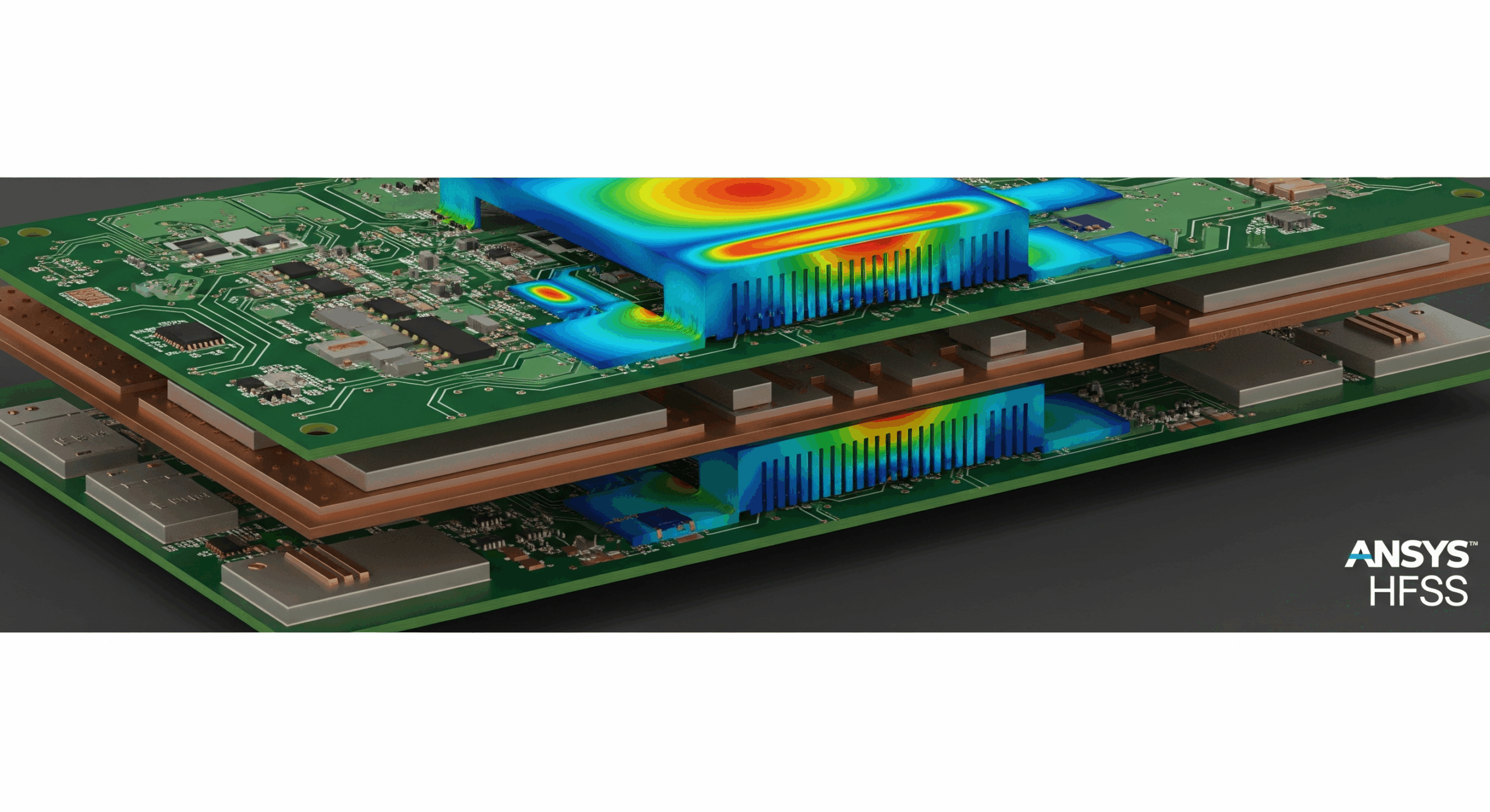
Printed circuit boards (PCBs) are at the heart of every electronic device. From smartphones to 5G networks, PCBs carry signals, connect components, and make systems run smoothly. As devices get smaller and faster, PCB design becomes harder. Engineers must deal with high frequencies, tighter layouts, and strict compliance standards. This is where ANSYS HFSS in India plays an important role.
ANSYS High-Frequency Structure Simulator (HFSS) is a powerful HFSS electromagnetic simulation software used by engineers worldwide. It helps in designing and analyzing the electromagnetic behavior of electronic components, including PCBs. In ANSYS HFSS in India, engineers use this tool to predict how electromagnetic waves will interact with their PCB designs. This allows them to identify and fix potential problems early in the design process, saving time and resources.
Using HFSS software for PCB offers several advantages for optimizing PCB performance:
HFSS uses advanced numerical methods to provide highly accurate predictions of electromagnetic behavior. This includes signal propagation, impedance matching, and radiation patterns.
By simulating the PCB design before it’s physically built, engineers can identify potential issues like signal reflections, crosstalk, and electromagnetic interference (EMI).
HFSS allows engineers to easily test different design variations and component placements to find the optimal configuration for performance.
Identifying and fixing issues through simulation reduces the need for multiple expensive physical prototypes.
Optimizing PCB performance with HFSS leads to more reliable and efficient electronic devices.
How to improve PCB performance using ANSYS HFSS involves focusing on several critical aspects of the design:
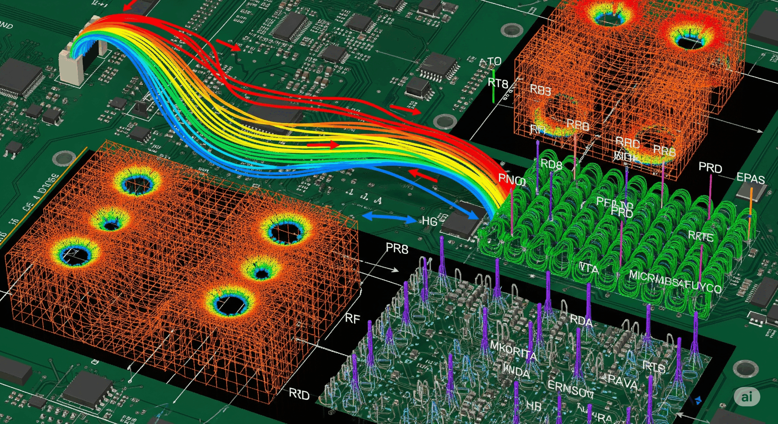
In high-speed digital circuits, maintaining signal integrity is crucial. Signal integrity refers to the quality of the electrical signals as they travel through the PCB traces. Issues like reflections, ringing, and distortion can occur due to impedance mismatches and discontinuities. ANSYS HFSS for high-speed PCB design optimization helps analyze these effects by simulating the transmission lines and connectors on the PCB. Engineers can then adjust trace geometries, impedance matching networks, and termination strategies to ensure clean and reliable signal transmission. This is a key aspect of electronic design automation (EDA).
For PCBs that operate at radio frequencies (RF) and microwaves, such as those used in wireless communication and radar systems, precise control over electromagnetic fields is essential. ANSYS HFSS for RF and microwave PCB circuits allows engineers to design and analyze critical components like transmission lines, filters, amplifiers, and antennas. By simulating the electromagnetic fields, engineers can optimize the performance of these circuits for parameters like insertion loss, return loss, and bandwidth. ANSYS HFSS antenna design capabilities are particularly valuable for optimizing the radiation patterns and efficiency of antennas integrated into PCBs.
EMI refers to unwanted electromagnetic energy that can interfere with the operation of electronic devices. EMC is the ability of a device to function correctly in its electromagnetic environment without causing or being susceptible to unwanted interference. EMI/EMC compliance testing is a critical part of product development. HFSS electromagnetic simulation helps predict and mitigate potential EMI/EMC issues early in the design cycle. Engineers can analyze radiation from PCB traces, coupling between different parts of the circuit, and the effectiveness of shielding techniques. This proactive approach helps reduce PCB design errors with ANSYS HFSS and ensures that the final product meets regulatory standards.
Many modern electronic devices include integrated antennas for wireless communication. Optimize 5G PCB antenna performance with ANSYS HFSS is increasingly important due to the higher frequencies and complex requirements of 5G technology. HFSS allows engineers to simulate the performance of on-board antennas, taking into account the effects of the surrounding PCB components and enclosure. This enables them to optimize antenna parameters like gain, bandwidth, and radiation pattern for efficient wireless communication.
While HFSS is primarily known for its high-frequency electromagnetic simulation capabilities, it can also be used to analyze power integrity in PCBs. Power integrity refers to the quality and stability of the power supply delivered to the active components on the PCB. Issues like voltage drops and power supply noise can affect the performance and reliability of the circuit. HFSS can help analyze the impedance of the power distribution network and identify potential problems.
The demand for high-performance electronic devices is constantly increasing in ANSYS HFSS in India. As a result, more and more companies are adopting advanced simulation tools like HFSS to optimize their PCB designs. Several ANSYS HFSS distributor in India for PCB design support this growing need by providing access to the software, training, and technical support. This makes HFSS simulation India a key enabler for developing cutting-edge electronic products.
To effectively use HFSS for PCB optimization, consider these best practices:
Accurate Modeling: Create a detailed and accurate 3D model of your PCB design, including all components, traces, and materials.
Appropriate Boundary Conditions: Apply the correct boundary conditions to your simulation to accurately represent the operating environment of the PCB.
Proper Mesh Generation: Generate a suitable mesh that accurately captures the geometry and electromagnetic field variations in your design.
Validation with Measurements: Whenever possible, validate your simulation results with physical measurements to ensure accuracy.
Iterative Design Process: Use HFSS as part of an iterative design process, where you simulate, analyze, and refine your design based on the simulation results.
Understanding Ansys HFSS related to PCB design enhances the overall design process:
electromagnetic field simulation: The core capability of HFSS, allowing visualization and analysis of electromagnetic interactions.
high-frequency PCB design: Designing PCBs that operate effectively at high frequencies, where signal integrity and electromagnetic effects become more significant.
RF & microwave circuit simulation: Simulating the behavior of circuits operating in the radio frequency and microwave spectrum.
signal integrity analysis: Evaluating the quality of electrical signals as they propagate through the PCB.
EMI/EMC compliance testing: Ensuring that the PCB design meets regulatory standards for electromagnetic emissions and susceptibility.
5G device design simulation: Utilizing simulation tools to design PCBs for next-generation 5G wireless devices.
PCB layout optimization tools: Software and techniques used to improve the physical arrangement of components and traces on a PCB.
virtual prototyping for PCBs: Using simulation to create virtual prototypes of PCBs, allowing for early testing and design validation.
These semantic keywords represent the broader context of using best software for PCB electromagnetic simulation in India like ANSYS HFSS and highlight its importance in modern electronic product development.
Optimizing PCB performance is critical for creating reliable and efficient electronic devices. ANSYS HFSS in India provides engineers with a powerful toolset to simulate and analyze the electromagnetic behavior of their PCB designs, leading to significant improvements in signal integrity, RF performance, and EMI/EMC compliance. By adopting best practices and leveraging the capabilities of HFSS, companies can reduce PCB design errors with ANSYS HFSS and bring high-quality products to market faster. For expert support and solutions in electromagnetic simulation and PCB design, consider partnering with Corengg Technologies.

EV Battery thermal simulation software. Electric vehicles (EVs) are the

CAD Design Software Guide for Businesses in 2026 | Corengg

Choosing the right ANSYS Partner in India is important for

Corengg Technologies is proud to announce its official partnership with

simulation software services The demand for clean and renewable energy

Aerospace engineering simulation software The aerospace industry builds machines that
